Perovskite image sensor catches 3x more light, could transform cameras, medical imaging
InnovationApart from cameras, the perovskite sensor is ideal for medical diagnostics and automated monitoring in agriculture and environmental systems.
Published:
Researchers in Switzerland have created a new perovskite-based image sensor that outperforms conventional silicon sensors in nearly every category, including light sensitivity, resolution, color accuracy, and adaptability for machine vision.
The innovative sensor, which reportedly holds the potential to revolutionize not only digital photography but also medical diagnostics and environmental monitoring, was developed by Maksym Kovalenko, PhD, a professor of functional inorganic materials at ETH Zurich, and his research team.
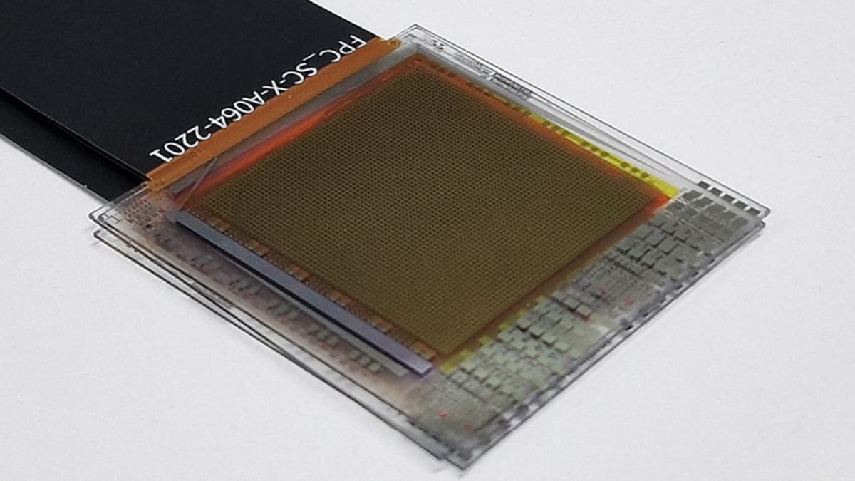
For the study, Kovalenko’s team collaborated with experts from the Swiss Federal Laboratories for Materials Science and Technology (Empa) to design and fabricate two fully functional thin-film prototypes.
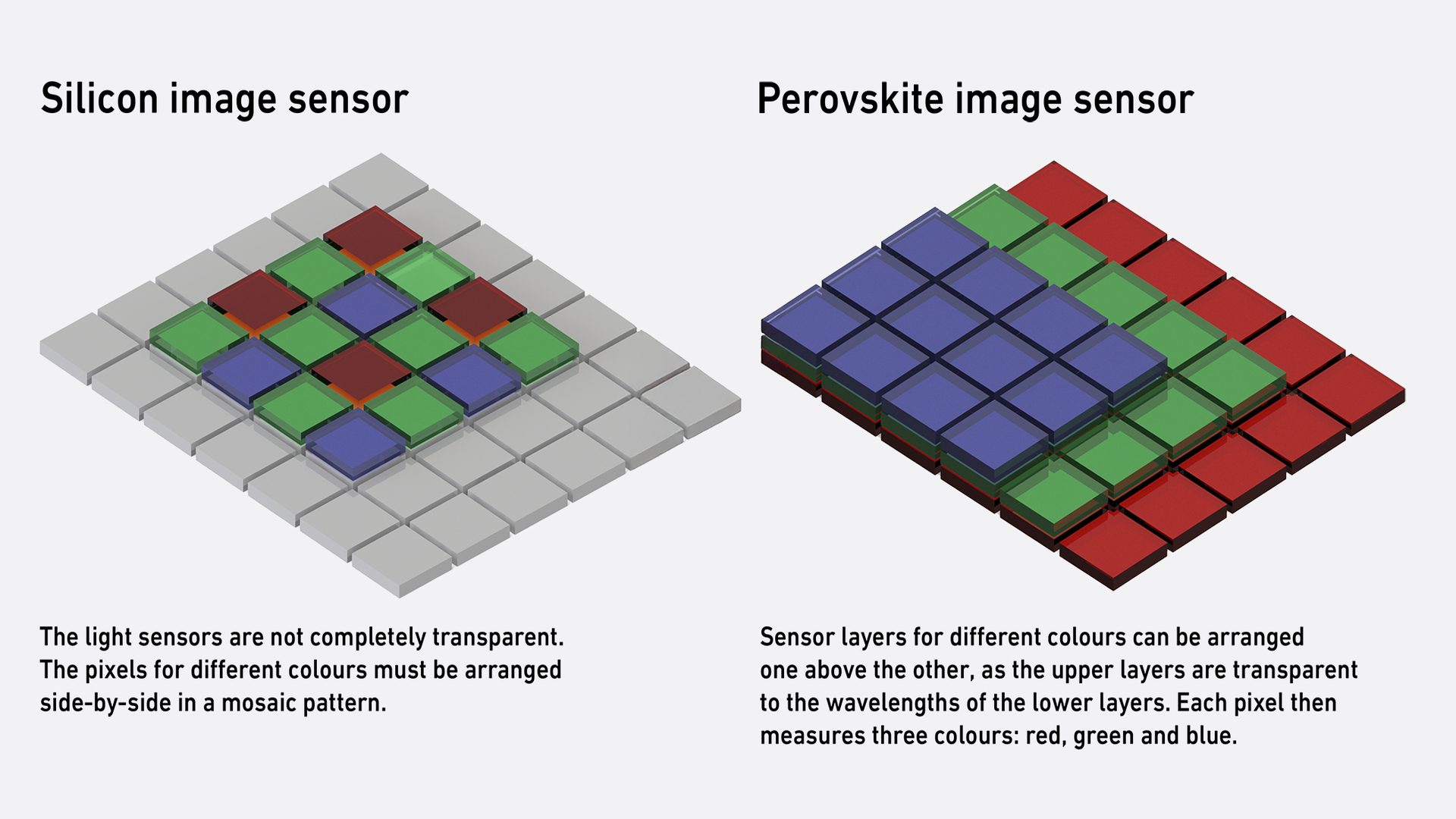
Unlike traditional sensors that rely on filters to detect color, which ultimately results in significant light loss, the new designs use stacked perovskite layers, each tuned to absorb a specific portion of the visible spectrum.
This unique mechanism allows each pixel to capture the full range of incoming light, thus significantly enhancing image clarity and color precision while reducing common digital artifacts.
Advertisement
A novel technology
Silicon has dominated the image sensor industry for decades, powering nearly every smartphone and digital camera and distinguishing colors in a way similar to the human eye.
However, traditional silicon sensors have a fundamental limitation as they use color filters to separate red, green, and blue (RGB) light, which means each pixel captures only about one-third of the available photons. This ultimately reduces efficiency and image quality.
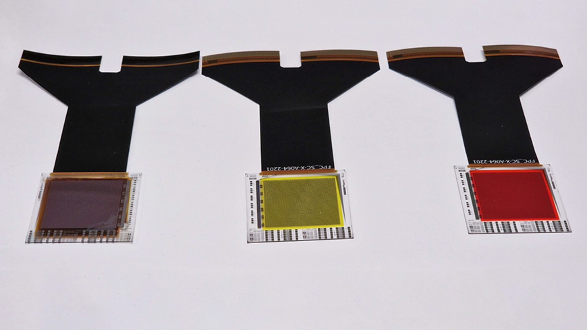
Red, green, and blue: The layers of the perovskite image sensor are transparent to the other wavelengths and can be stacked without losing light. Credit: Empa / ETH Zurich
To overcome these challenges, Kovalenko and his team came up with a novel perovskite sensor that uses stacked pixels capable of absorbing every photon of light for color recognition without the need for filters.
The innovative tech is made out of a crystalline material called lead halide perovskite, a semiconductor whose light absorption properties can be tuned by tweaking its chemical composition.
How it works
In contrast to silicon, the perovskite is much easier to process, and its physical properties change depending on its chemical composition, a trait the researchers used to build the new sensor.
By adjusting the mix of iodine, bromine, and chlorine ions in the perovskite crystal, researchers can target specific wavelengths of light, while allowing other wavelengths to pass through.
For example, if the perovskite contains more iodine ions, it absorbs red light. To absorb green, the researchers add more bromine, and for blue, more chlorine, all without the need for filters.
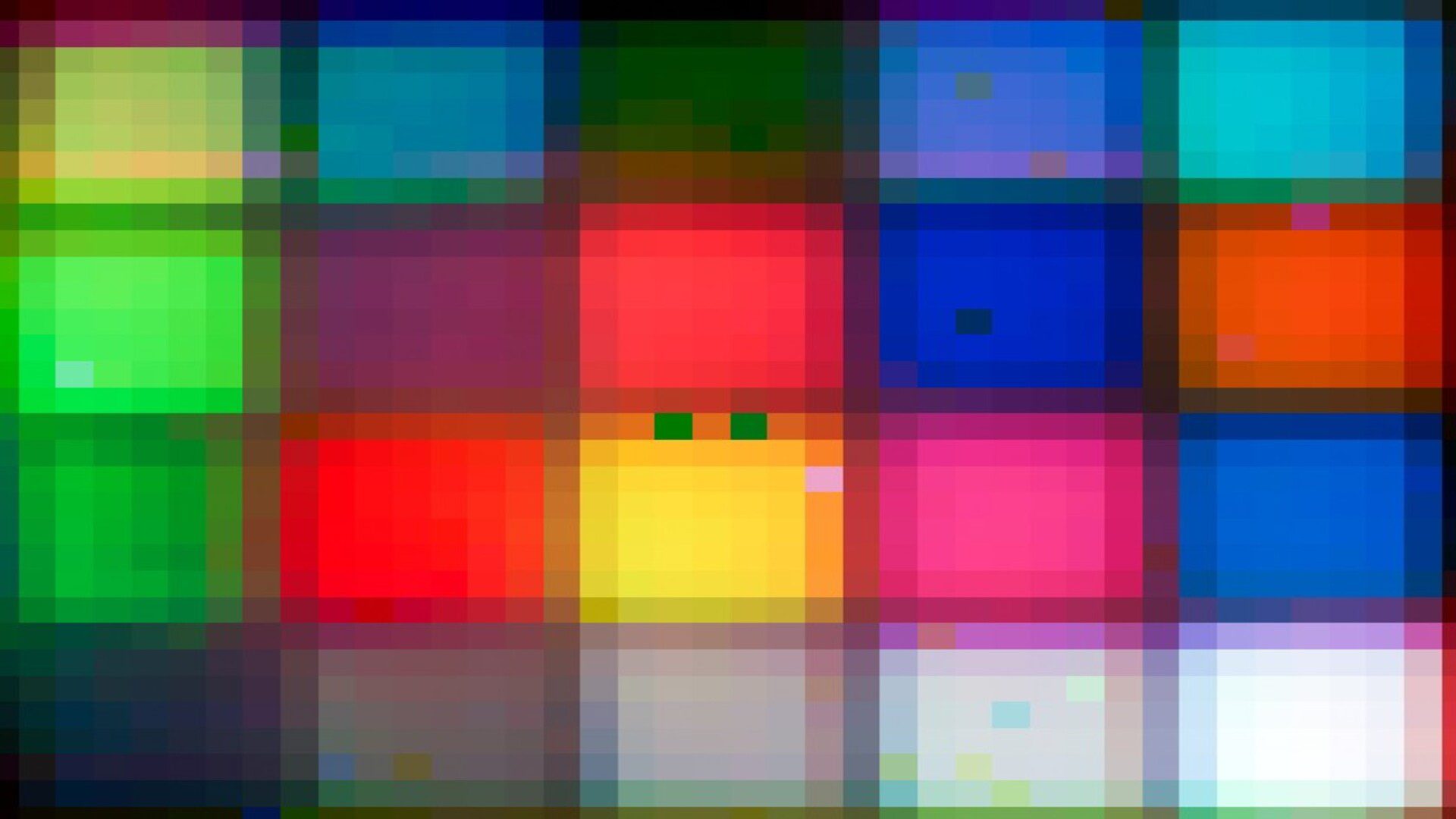
A color palette imaged with a prototype perovskite sensor. Precise color reproduction is one of the strengths of the new technology. Credit: Empa / ETH Zurich
The design allows perovskite-based image sensors to potentially capture three times more light than conventional sensors of the same size, while also offering three times greater spatial resolution.
Kovalenko and his team previously demonstrated this concept with large single-crystal pixels, but now, for the first time, they have miniaturized the technology using thin-film fabrication techniques.
“We are developing the technology further from a rough proof of principle to a dimension where it could actually be used,” Kovalenko said, explaining how the first transistor was made of a large piece of germanium with a couple of connections. “Today, 60 years later, transistors measure just a few nanometers.”
Advertisement
Looking ahead
The two prototype sensors developed by the group differ in their readout technology, through their paces, but both validate the concept. The team believes they’ve reached industry-relevant thickness and demonstrated the technology’s scalability.
What’s more, consumer digital cameras are not the only field where the new image sensors can be used. Thanks to the material’s unique properties, they are also well suited for machine vision applications.
According to Sergii Yakunin, PhD, a lecturer at the department of chemistry and applied biosciences at ETH Zurich, and one of the study’s co-authors, perovskite sensors offer a key advantage in hyperspectral imaging, as each layer can be precisely tuned to absorb a specific wavelength range.
Perovskite image sensors can, in theory, capture three times as much light as conventional image sensors of the same surface area while also providing three times higher spatial resolution. Credit: Sergii Yakunin / ETH Zurich / Empa
While the current prototypes have pixel sizes ranging from 0.5 to 1 millimeter, which is much larger than the micrometer-scale pixels in commercial sensors, the researchers believe perovskite pixels can be made even smaller than those in silicon-based devices. Achieving this will require a redesign of supporting electronics, which are currently optimized for silicon’s material properties.
RECOMMENDED ARTICLES
“It should be possible to make even smaller pixels from perovskite than from silicon,” Yakunin said, explaining that the electronic connections and processing techniques need to be adapted for the new technology.
“Today’s readout electronics are optimized for silicon,” Kovalenko concluded in a press release. “But perovskite is a different semiconductor, with different material properties.”
The study has been published in the journal Nature.
ABOUT THE AUTHOR
Georgina Jedikovska Georgina Jedikovska, journalist, plant engineer, oenophile and foodie. Based in Skopje, North Macedonia. Holds an MSc. degree in Horticultural Engineering, with a specialization in viticulture and oenology. Loves travelling, exploring new cultures, a good read, great food and flavorful wines. Enjoys writing about archaeology, history, and environmental sciences.
NEWSLETTER
The Blueprint Daily
Stay up-to-date on engineering, tech, space, and science news with The Blueprint.